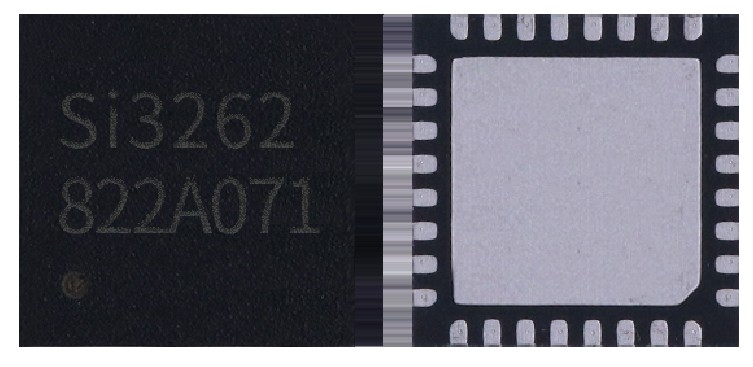
SI3262 — Highly Integrated Low-Power RISC-V + 13.56 MHz NFC Reader SoC
The SI3262 is a highly integrated low-power SoC that combines a RISC-V-based low-power MCU with a 13.56 MHz contactless reader module.
The MCU module features low power consumption, low pin count, and wide voltage range, integrating a 13/14/15/16-bit ADC, LVD, UART, SPI, I²C, TIMER, WUP, IWDG, RTC, TSC, and other rich peripherals. The core uses a RISC-V RV32IMAC.
The reader module supports ISO/IEC 14443 A/B protocols and Automatic Carrier Detection (ACD). No external circuitry is required; the internal transmitter directly drives the reader antenna to communicate with ISO/IEC 14443 A/B cards and transponders. The receiver module provides a robust and efficient circuit for demodulating and decoding signals from ISO/IEC 14443 A/B compatible cards and transponders. The digital module handles complete ISO/IEC 14443 A/B framing and error detection (parity and CRC). In ACD mode, the reader module stays in sleep most of the time and is periodically woken by a 3K RC timer to detect a 13.56 MHz RF field or card with extremely low power. Upon detection, it automatically generates an interrupt to wake the MCU. Field and card detection can be enabled separately. The entire ACD process requires no MCU intervention.
In addition, the product is supplied with mature debugging and development software and rich function libraries, which can significantly lower the development threshold and shorten the development cycle.

MCU Module Features
Built-in RISC-V RV32IMAC core
Maximum operating frequency 32 MHz
4 kB SRAM
32 kB embedded Flash + 4.5 kB NVM (≥100,000 erase/write cycles)
1× SPI Master
1× I²C Master
2× UART supporting up to 1 Mbps
2× advanced timers (Timer1 with 4 complementary PWM outputs)
64-bit SysTick (MTIME), not for timekeeping
Fast high-precision 13/14/15/16-bit ADC with integrated 1.2 V reference
Wide ADC input voltage range: 0–4.8 V (must not exceed VDD_MCU)
10 ADC input channels (8 external)
Built-in low-voltage detection (LVD)
Up to 15 GPIOs with external interrupt support
Integrated capacitive touch detection module (TSC), up to 15 channels
PA10 usable for BOOT configuration
Hardware watchdog
1× RTC for timekeeping
1× WUP
4 low-power modes, minimum <0.6 μA (watchdog active)
32-bit true random number generator
cJTAG 2-wire debug interface
Operating voltage range: 1.8–5.5 V

Reader Module Features
Highly integrated analog circuitry for demodulation and decoding
Buffered output drivers requiring minimal external components for antenna connection
Supports ISO/IEC 14443 A/B
Operating distance in reader mode depends on antenna size and turns; typical 50 mm
Supports ISO/IEC 14443 A/B high-speed communication up to 848 kBd
Supported host interfaces:
SPI up to 10 Mbit/s
I²C fast mode up to 400 kBd, high-speed mode up to 3400 kBd
Serial UART up to 1228.8 kBd
64-byte FIFO
Flexible interrupt modes
Low-power hard reset function
Software power-down mode supported
Integrated programmable timer
27.12 MHz internal oscillator
Supply voltage 2.5–3.6 V
Integrated CRC co-processor
Programmable I/O pins
Supports ACD mode:
Automatically detects 13.56 MHz RF field and cards
ACD process requires no MCU intervention
Oscillator start-up failure monitoring
Other Features
Ultra-low power consumption, minimum 1.7 μA (MCU in power-down, reader in hard power-down)
Typical ACD mode consumption 4.1 μA (MCU in power-down, reader card-search interval 500 ms)
Operating temperature range –40°C to +85°C
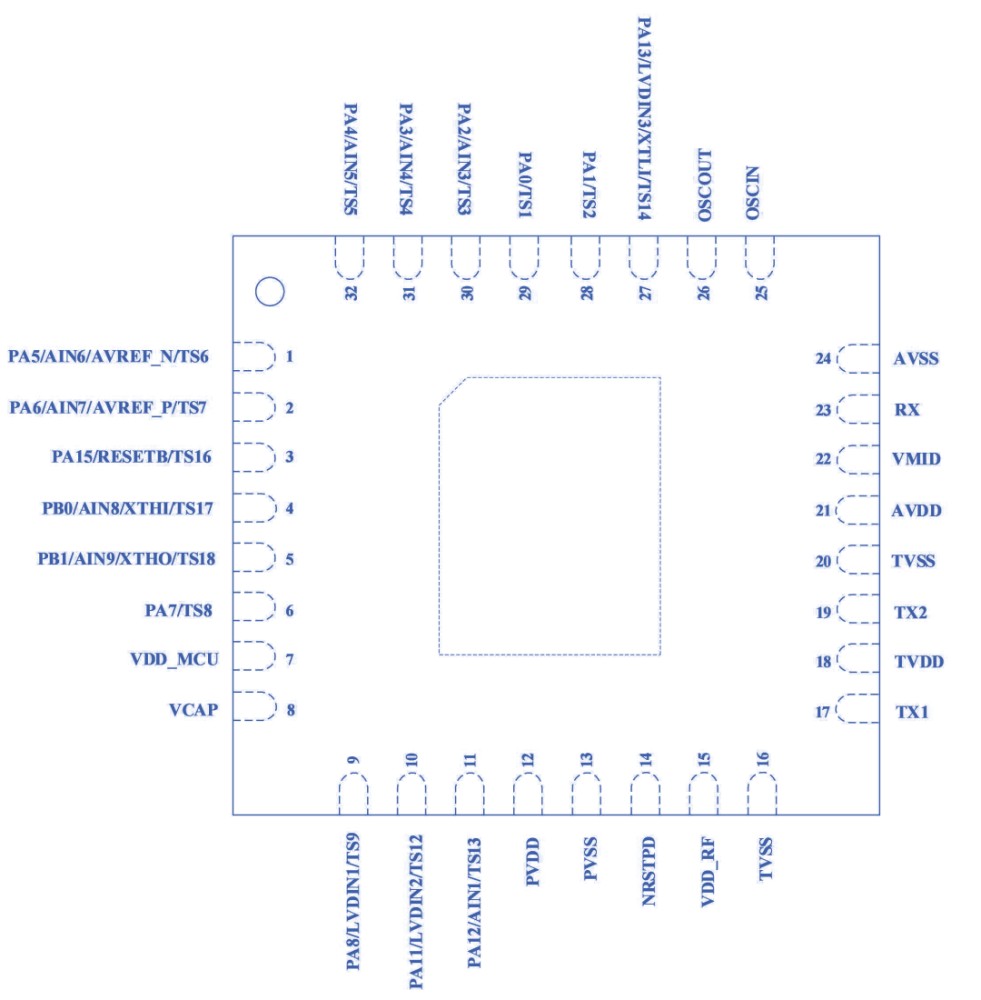
QFN0505-32L 5×5 mm package
Extremely few external components, reducing system cost
Supplied with mature debugging and development software and rich function libraries to significantly lower the development threshold and shorten development cycles


.png)

.png)


